Back in the summer I was lucky enough to finagle my boss into letting me take Dmitry Nedospasov (@nedos)’s hardware hacking training. In it I cut my teeth on using an FPGA to interface with target hardware. After implementing a UART we implemented a module that could parse part of Apple’s OneWire, used to negotiate power exchange, among other things, with your iPhone over the lightning cable. Our ‘final project’ was to build a UART-controllable glitcher, using it to try to glitch a development board.
While we got it working, it was with a bit of hand-holding from Dmitry, including setting up the scope, the power supply etc. In an effort to concretize the knowledge, I decided when I got home that I wanted to do it again on my own.
If you haven’t noticed, hobbyist FPGAs have flooded the market. In 2015 Lattice’s iCE40 series FPGA had its bitstream format reverse engineered, spawning an explosion of open source tooling for synthesizing, place and route, and simulation. Altera’s (Intel’s) and Xilinx’s bit stream format have not been reverse engineered, and so you are stuck using their tools if you decide to develop on those boards. I’ve played around with a few boards, and the iCEBreaker is my recent favourite. The people on their Discord are super helpful, the toolchain is excellent, and the board itself is great for the price.
Porting it over wasn’t too much work, the only real difference was that the FPGA we used in training was a Digilent Arty, which has a 100MHz clock, while the iCEBreaker’s has a 12MHz. This requires we change anything that’s counting cycles to account for the 8.33x slower clock, and we lose some granularity in anything we want to count (since each clock cycle has a longer duration). This is also an opportunity to generalize some of the code to not make as many assumptions about the FPGA it’s running on. Because I was rusty, I chose to try to ‘blindly’ re-write some of the modules, instead of using the code Dmitry has on his github.
Background
I can’t really give a better background to this than Dmitry does in his blog post about it. In short, when the target board boots up the bootROM reads the flash, and depending on the value it reads from address 0x2FC, and the state of a few pins, it determines whether the UART goes to a sort of shell, and whether you can use this shell to read out the flash. This is intended so that you can develop your firmware and debug in the bootloader, but then flash a version that sets this value when your firmware is production ready, hopefully preventing the end user from dumping it from the flash. The vulnerability here is that it’s a 4 byte value, and only a specific value (0x12345678) will lock the bootloader in the expected way. That means that if any of the 32 bits read here are read incorrectly, the bootROM will consider the device unlocked. This is opposed to, for example, requiring a specific value to unlock the bootloader, and having the other 4 billion values lock it.
If we can get the CPU to misread the flash at the very moment it happens to be reading that value, then we can have it jump to the bootloader in the unlocked state. It’s as easy as that! (Famous last words)
The idea here is that we will use the FPGA as a tool that goes between my host machine and the target board. We can communicate with it using UART, and certain special bytes are interpreted as commands for the FPGA, while other values are simply passed through to the target board (to talk to its bootloader). The values sent back from the target board are simply passed directly through to the host machine. The FPGA supports configuring the delay between resetting the target board and pulsing a ‘glitch voltage’, and how long that glitch pulse lasts. It also supports sending multiple pulses, and of course can reset the target board and activate the glitch.
We use an FPGA here instead of a microcontroller for a few reasons:
- First, because we can configure things at the clock level, we can have very specific timing (1s/12000000 = 83.3ns precision).
- Second, for the same reason, we don’t have to worry about jitter: With a raspberry PI we’d worry about the OS scheduling other process and such, contributing to inconsistency between runs. Even with an Arduino or other microcontroller, with no operating system, we’d have to worry about interrupts messing up the timing.
- Third, I wanted to get more practice writing Verilog and using an FPGA.
Setup
For the toolchain, I mostly took everything from WTFpga, which is a beginner’s lab that uses the iCEBreaker board. It uses Yosys, nextpnr, and a few tools from project icestorm. These are all open source tools that you can invoke from the command line, you don’t need a GUI (so I don’t need to run Vivado in a VM) and the time to build is much, much faster than the few minutes it takes to get a synthesis to fail with obscure errors in Vivado. This really sped me up because I am not disciplined and instead of inspecting my code for errors ahead of time, I tend to compile, patch, and iterate until it builds.
For debugging I used PulseView (part of sigrok) when debugging real signals, and GTKwave to look at my simulated waveforms.
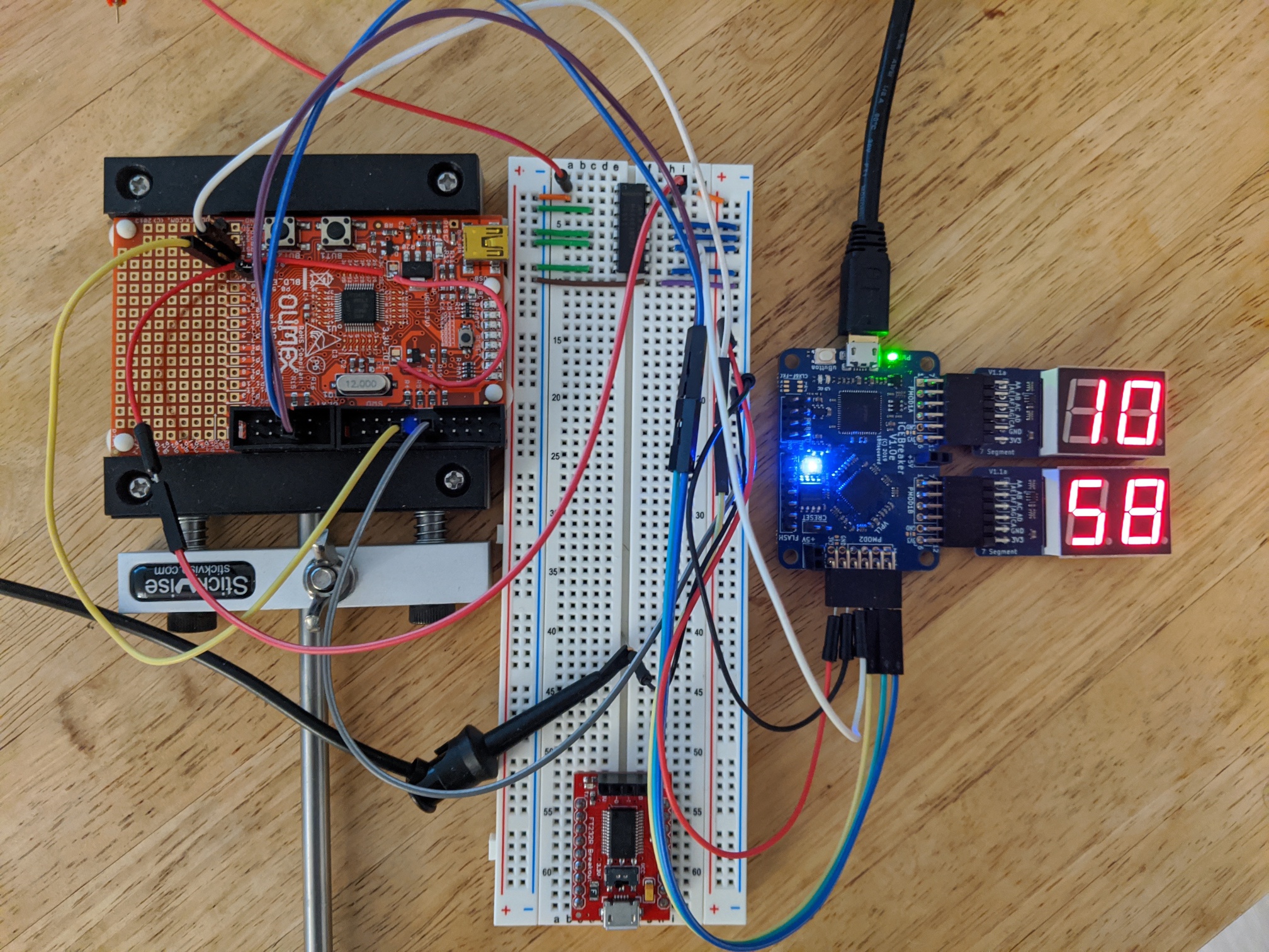
For hardware, I obviously used the iCEBreaker, as well as the Olimex target board. My bench top supply is a DC50V5A, a cheap but handy configurable buck converter I got on Ali express. While I have a Saleae, I prefer Sigrok, and at the speeds I was running things at, a cheap 24MHz logic analyzer was enough. In the end I had some troubles debugging something using that alone and borrowed an oscilloscope, but in hindsight it wasn’t necessary, just nice to have.
Design
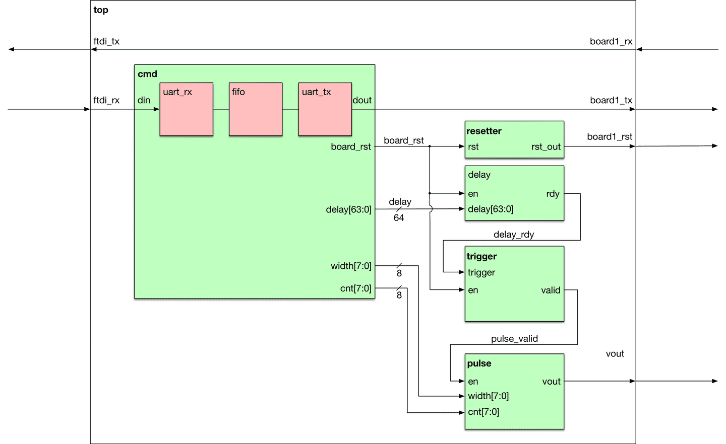
Again, I am just porting over Dmitry’s design, so here’s the block drawing stolen from his blog:
The tl;dr:
- The
cmdmodule intercepts everything the host computer sends over UART. Based on the first byte it either interprets it as a command for the FPGA, or passes it through to the target. - The
resettersimply holds the reset line down long enough for the target to reset (instead of one cycle). - The
delaymodule starts counting on reset and waits the configured number of cycles before sending its own signal. - The
triggermodule waits for the delay to finish and then tells the pulse module to send a pulse. - The
pulsemodule is a lot like the delay module, except that it uses a different config, and its output is connected to the power multiplexer.
This is all controlled by a python script that talks to the UART, first configuring the FPGA, then activating a glitch, and then communicating with the target. It determines whether it can read out the flag, and if it can’t, it adjusts the delay and pulse width configs and tries again.
The FPGA has two inputs: The UART from the host, and the UART from the target board. It has 4 outputs: The UART to the host, the UART to the target board, a reset line to reset the target, and a vout that is used to control the analogue multiplexer, to quickly drop the voltage powering the target board.
Testing
While you can certainly test on a real FPGA, it’s very difficult to see what’s going on inside the FPGA. You can blink LEDs, or, if you have the hardware, use seven segments displays to output whatever relevant value. I found this very handy and ended up buying a second just so that I could tell both my pulse width and delay count at a glance.
That said, even with the rather quick tools, flashing and debugging with a logic analyzer is a lot slower than ideal. I suggest setting up a good test bench and run simulations.
Simulation
I used Icarus Verilog to simulate the various modules, and GTKWave to look at the waveforms it generates. The basic idea is that you write extra verilog that simulates the inputs to your top module, and then verify that behaviour of the internal signals are as expected. As opposed to running on real hardware, it’s easy to introspect any internal value any any point in time. You can also write test benches for any individual module, ensure that each part is behaving as expected before combining them together.
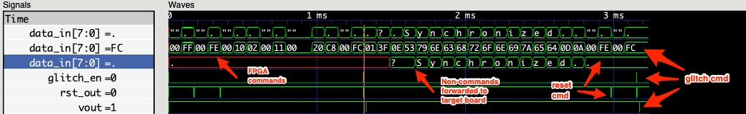
Here we see my simulation of the whole glitcher, I send a few configurations, and then some commands that should be passed through to the target.
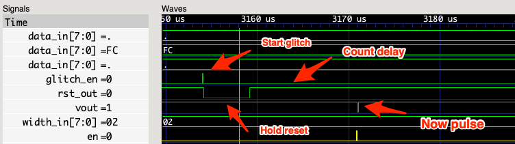
And here is what happens when the glitch command is sent. We see the reset line go down, then there is a delay based on the delay configuration we previously set, and the vout line goes low for a period of time determined by the pulse width configuration.
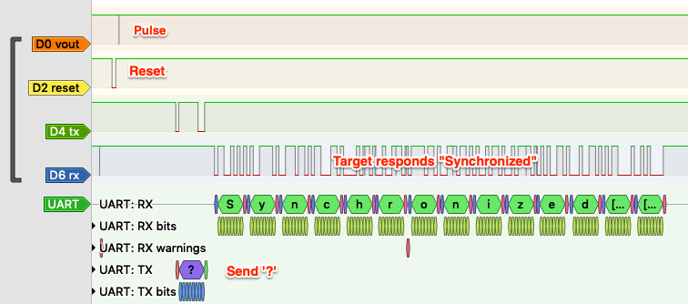
While a simulation is good, the real test is when you see it work on real hardware, which I was able to see here with my logic analyzer:
Troubles
The Olimex board actually runs faster than my FPGA, and in training our FPGA was more than 8 times faster. In practice our successful glitch had a very short pulse, in the tens of cycles (at 100MHz). With a 12MHz clock (I thought) I was in trouble. There is significantly less granularity in pulse widths, and we risk the ideal pulse width between somewhere between a n cycles and (n+1) cycles.
I tried to fix this by using a PLL which allows you to generate a clock that is faster than the input clock by some multiple. Again, icestorm to the rescue here, I was able to use icepll to generate most of the code needed to generate a 48MHz clock from a 12MHz input.
I kept most modules on the main clock, but fed my new fast_clk to the pulse module. I adjusted my testbench to generate the faster clock and was able to verify that I could generate shorter pulses (with four times the granularity). I actually found a bug in my pulse module here: Since my pulse module was running on a clock four times faster than the rest of the system, including the module that enables the pulse, with short width values my pulse was ending before the enable signal was unset. This was causing the pulse module to immediately start a second pulse. I fixed this by adding an extra state to the module that made it wait until after the enable signal was unset before returning to the waiting state.
Unfortunately, when I ran this on real hardware, I found that my pulse width seemed to be consistently the same value. I was unable to debug this and decided to see if I could get the glitch to work without the finer granularity (spoiler: I could).
Running it in real life
Once I had my simulation looking good, and I was able to see that the behaviour in the real world looked like what I was expecting, it was time to actually glitch the board.
Modifying the board
To have the CPU misread the lock value we want the voltage to drop at precisely the time when it’s reading the appropriate address from flash. Because there are decoupling capacitors on the board, which would smooth out any abrupt voltage change and make this a lot more difficult, I had to remove those capacitors. I also cut traces between the board’s voltage regulator and the VCC and VCCIO, so that it’s powered exclusively from the output of my analogue multiplexer. This is all well documented in the third part of Dmitry’s blog series.
Determining the supply voltage
Because we don’t live in a frictionless vacuum where infinitely fast changes in voltage are possible, even without decoupling capacitors the CPU won’t see an instantaneous change in voltage when we toggle vout. Because of this, we want to minimize the time the voltage change happens, and so we run the board at the lowest voltage we can find where the board behaves normally.
For me this was 2.30V, which I determined by running a loop where I continuously reset the board and then tried to communicate with the bootloader. I adjusted the voltage on my benchtop supply while this was running until it was just barely high enough to reliably read “Synchronized” after sending the “?” bootloader command. The glitch voltage for my setup was simply 0V, but this was mostly due to me only having a single channel power supply. You might be able to more reliably reproduce the glitch if instead of glitching between X and 0 you glitch between X and Y, but if I got it to work with 0V, you can, too.
The moment of truth
I hooked up the reset line of my FPGA to the reset on the board, hooked up vout to the control pin of the multiplexer, tied Vglitch to ground, and then tied Vcc to the 2.3V I determined as the minimum stable voltage.
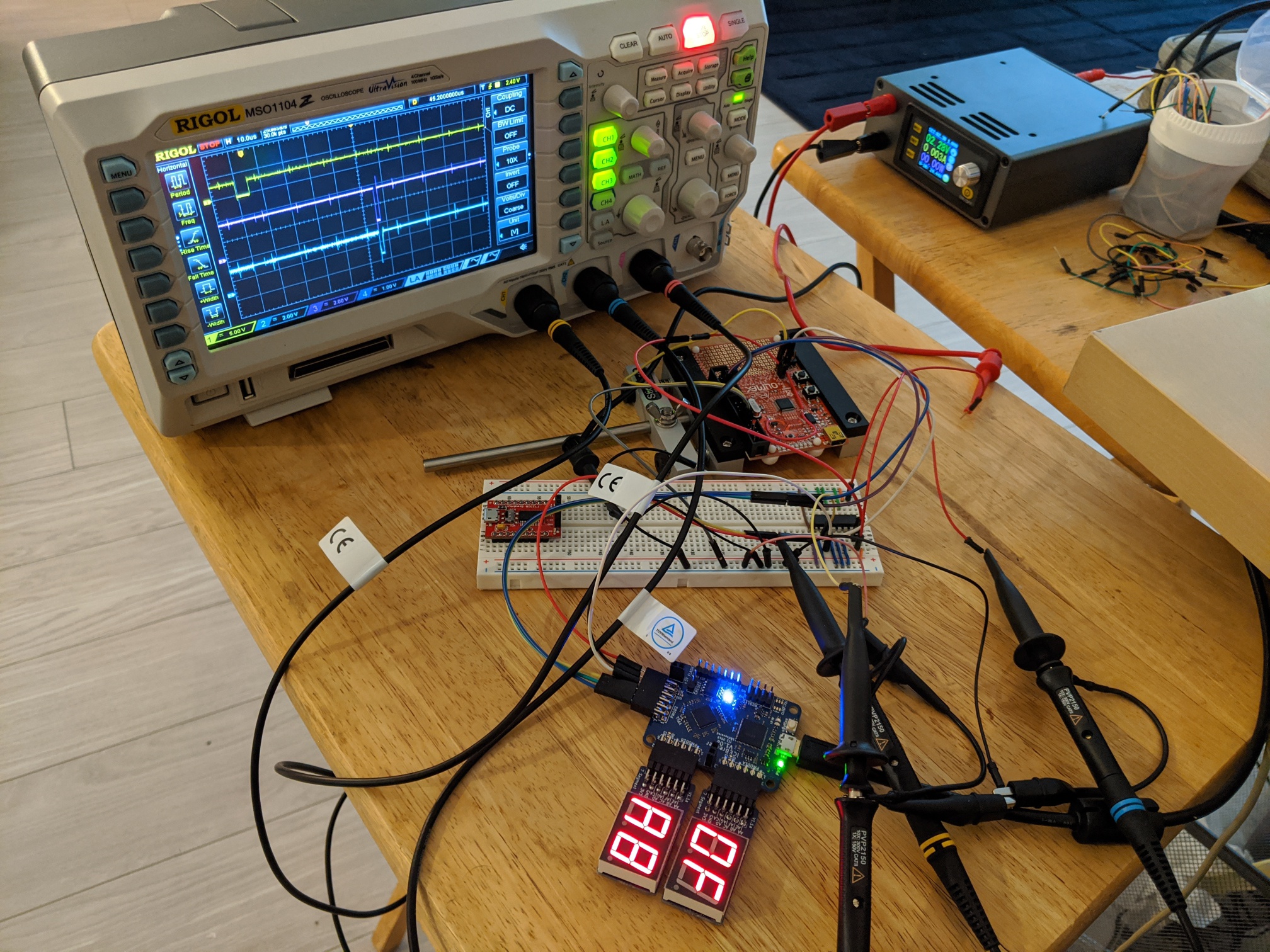
A friend from work let me borrow his oscilloscope, so I was able to see in real time the reset signal followed by the vout signal pulsing and the corresponding voltage drop in Vcc.
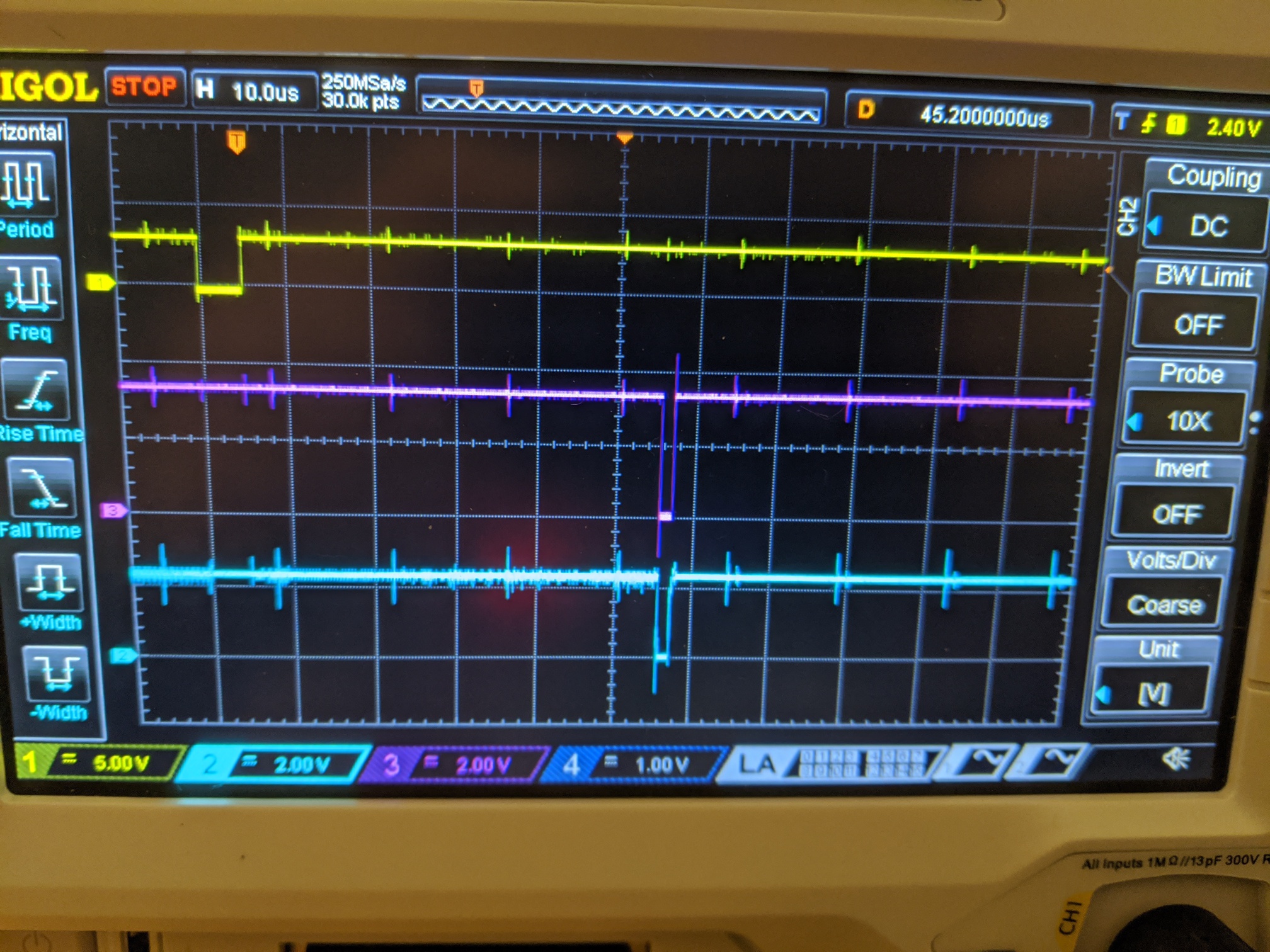
The yellow line is the reset signal, which is held low for 5uS, and then vout, the cleaner purple signal, is toggled delay cycles later, for pulse width cycles. The cyan signal is the actual voltage seen, which we can see is ‘dirtier’ than the purely logic-level vout signal.
Given enough time you can basically brute force any combination of delay and width, but knowing that the board boots in under 100uS and knowing that with pulses too wide we never get a stable system I played with delays between 60 and 1200 cycles (5uS to 100uS) and pulses between 1 and 25 cycles.
I then ran my script, which brute forced through the range of delay and pulse width values until I was treated to a nice dump of the flash I was not supposed to read! You can see in the video below that the width of the pulse get wider until it reaches its max, at which point the delay is incremented and the width values are all tried again.
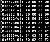
And with a certain width and delay (15 and 680 in my case) our script dumps out the flash!
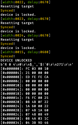
If we look at the lock value at 0x2fc, we see that it’s 0x12345678 as we expect:
We don’t see a glitched out value because this dump is after we’ve glitched the bootloader, with the voltage back at its stable value. At this point in time the bootloader has already (incorrectly) determined that the bootloader is unlocked, and so all subsequent reads succeed. We don’t know exactly what happened during the glitch: The read could have misread the value from flash, the comparator could have mis-behaved, the conditional flag could have not been set, the jump instruction could have been skipped, or countless other weird things. What we do know, however, is that we got what we want: The bootloader running stably in a state where it thinks the flash isn’t locked down.
Of course in real life things didn’t go this smoothly, while testing it out I found a bunch of bugs, including how if my delay was too short it would send a pulse while the reset was still low and my pulse width counter had an off-by-one in counting its cycles, among other things, so don’t worry if you try this and have issues as well: Isolate the issue, make sure your simulation works, compare to real life, and debug.
Conclusions
I found this to be a really fun personal project. I find repetition key to remembering things, and so rewriting modules I had written months ago, relearning Verilog syntax, and hitting the same issues while debugging (hopefully) helped me to remember it for next time.
On the FPGA side, the open source tool chain I used for the FPGA stuff was very easy to use, and being able to quickly build both simulations and the real bitstream helped me iterate a lot more quickly. It was well worth my time to get my Makefile running nicely.
On the glitching side, I found that it really demystified the whole thing for me. If I can whip up something that is apparently precise enough to (sort of) reliably glitch a target board running in the dozens of MHz, I must be doing something right.
I wouldn’t have been able to do this without a lot of help from Dmitry. Even now months after taking his training he was willing to help me with whatever dumb questions I have. Seriously consider taking his training. I had Dmitry look at this post before publishing and he offered a discount code! So if you sign up use the code grazfather for 5% off!
Since I was simultaneously trying to figure out glitching stuff while also re-learning Verilog and trying to do it in a new ecosystem, I needed and received lot of help from the nice people on the 1bitsquared discord, so big thanks to them! If you’re looking for your own FPGA board, I can’t recommend the iCEBreaker enough!
My code is available on github, which includes the verilog to configure the FPGA, as well as the python script used to orchestrate everything. It’s heavily based on nedos’s own version.
Last modified on 2019-12-08